Design Review Guide
Contents
Design Review Guide#
Altium: PCB Review Pre-Checklist
Required
Validate project/schematic
Update PCB from schematic
Repour all polygons
Pass DRC (design rule check) with no errors
Altium PCB Filter#
Altium Designer Query Language
Check assembly text is oriented correctly
IsText and OnLayer('ASM Top') and (Rotation = 180000)
Find traces of desired widths on a given layer
(OnLayer('L1') or OnLayer('L2')) and IsTrack and (Width > 0.381)
Find unrouted pads on PCB
(Net='No Net') and (IsPad=True)
Simulation#
Altium: How to Simulate a PCB Design
Front-end PCB Simulation and Analysis
Impedance Calculations in PCB Stackup Design
Simulations During PCB Layout and Routing
Post-Layout Simulations
More Advanced PCB Simulations
Decoupling Capacitors#
Resource: Decoupling Capacitor Calculations
Use a combination of inrush current calculations and impedance spectrums to minimize PDN impedance
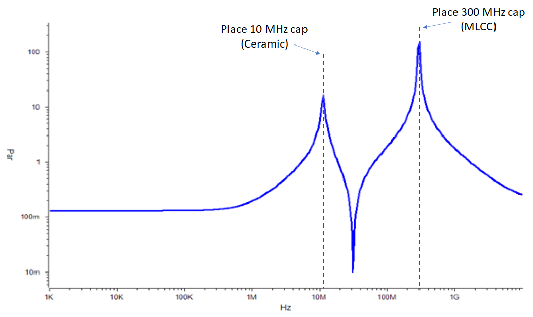
Fig. 10 PDN Impedance#
Vias#
Resource: Via Stitching & Via Shielding
Via Stitching
maintains low impedance and short return loops
Via Shielding
reduces crosstalk and electromagnetic interference in RF signals
provides low impedance path for EMI to travel, effectively grounding any stray signals that may be present
Power Distribution Network#
Goal is to ensure sufficient current and voltage to all loads.
Requirements:
Sufficient copper between sources and loads
Capacitor values and placement
VIAs sizes
Tools: