Discussions
Contents
Discussions#
Q1: Trace width#
PCB Trace Inductance and Width: How Wide is Too Wide?
Goal: minimize PCB trace inductance per unit length while keeping impedance constant
IPC 2142 formulas are only highly accurate within a particular impedance range
Waddell’s implementation produces less than 0.7% error which is much better than IPC-2141
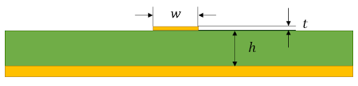
Fig. 7 Trace Geometry#
Q2: Filling unused area in signal planes with copper pours#
On Shaky Ground—the Arguments Against Copper Pours
Ground pours resemble patch antennas and can emit noise
When the copper is thick, desoldering and service operations are more difficult
Q3: Current sensor location#
Current Sensing: Where to Place the Sense Resistor
Placing sense resistor after inductor provides best signal to noise ratios. Ultimately, resistor should be replaced with hall sensor to improve dissipated power if it’s within budget ($).
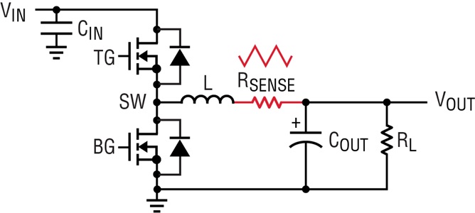
Fig. 8 Sense Resistor in Switch Mode Power Supply#
Q4: Gate driver protection#
Gate Resistor for Power Devices
Peak Current of Isolated Gate Drivers
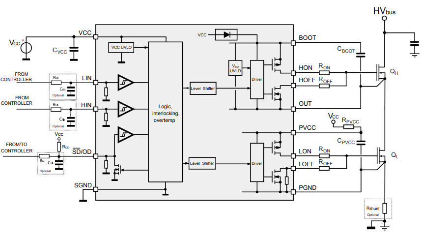
Fig. 9 Typical Application#
Design |
Component |
|---|---|
Gate Driver |
|
MOSFET |
Given gate driver specs, find in series resistance where \(R_G = R_g + r_g\).
\(R_g\) is the additional resistance added.
\(r_g\) is the MOSFET contact resistance.
\(V_{BO}\) |
Source |
Sink |
\(R_{\text{DS_on}}\) |
\(R_{\text{DS_off}}\) |
|---|---|---|---|---|
6.0V |
1.3A |
2.4A |
2.0\(\Omega\) |
1.2\(\Omega\) |
15V |
5.5A |
6.0A |
1.25\(\Omega\) |
0.9\(\Omega\) |
High Side Calculations
Low Side Calculations
Resistor Size
Additionally, power dissipated through the resistor is
for selecting components.